
Optii Technical Specification
Electrical Connection
The I2C Galvanic Isolation/Level Shifter 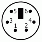 Optii has two Mini-DIN connectors for the connection of the two I2C buses. The figure shows the pin assignment of the male connector
| PIN | Description |
| 1 | SDA |
| 2 | TEST_IN |
| 3 | GND |
| 4 | Vcc |
| 5 | SCL |
| 6 | TEST_OUT |
Mechanical Specification
Mechanical Data (these values may differ)
- Height: 28 mm
- Width: 42 mm
- Length: 68 mm
- Material: blue plastic housing
- Weight: 50 g
Absolute Maximum Ratings
| Supply Voltage (Vcc) | -0.5 V to 6.0 V |
| Input Voltage I2C-lines | Vcc |
| Testpin Input | Vcc |
| Temperature Range | 0 °C to +40 °C |
| Sink Current (on Line) | 200 mA |
| Isolation Voltage | 2500 V |
Warning: Stresses beyond those listed may cause permanent damage to the device!
Power Supply Characteristics
| Min | Typ | Max | Unit | |
| Supply Voltage | 1.5 | – | 5.5 | V |
| Power Mode Switch Voltage | – | 2.5 | – | V |
| Power Mode Switching Hysteresis | – | 600 | – | mV |
| Power Dissipation (one Bus) | 40 | – | 100 | mW |
I2C-Line Characteristics
| Min | Typ | Max | Unit | |
| Max. Transfer Speed | 0 | – | 800 | kHz* |
| Propagation Delay | – | 50 | – | ns** |
| Capacity | – | – | 50 | pF |
| Sink Current | – | – | 200 | mA |
*) Accelerated Fast Mode (Fast Mode ist specified with 400 kbit/s only). This means that boosting, as specified for High-Speed Modes above 400 kbit/s, is not supported.
**) This is the delay between the detection of an active external device and the activation of the appropriate transducer on the other bus. The overall propagation delay depends on the bus capacity and the pull-up resistors.
Testpin Characteristics
| Min | Typ | Max | Unit | |
| Logic High Input Threshold | – | 0.85 | – | V |
| Logic Low Input Threshold | – | 0.4 | – | V |
| Logic High Output Voltage | – | – | Vcc | V |
| Logic Low Output Voltage | – | – | 100 | mV |
| Propagation Delay | – | – | 200 | ns |
Reference Voltage
Figure 2 shows Optii’s internal reference voltage for both power modes.
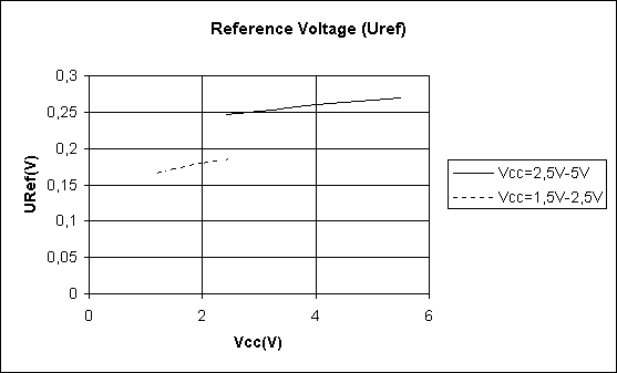
- Figure 2 Internal Reference Voltage Uref
Remaining Voltage
Figure 3 shows the remaining voltage if Optii pulls down an I2C line in dependency of the pull-up resistor Rp.
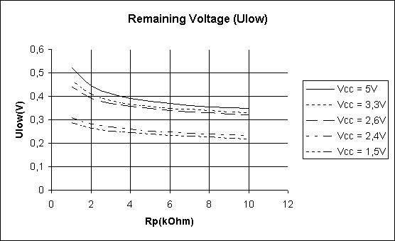
- Figure 3 Remaining Voltage Ulow
Supply Current
The necessary supply current for proper operation in dependency of the supply voltage is shown in Figure 4. This is the current for a single bus only.
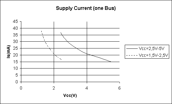
- Figure 4 Supply Current (Single Bus)
Power Consumption
The typical power dissipation of a single bus is shown in Figure 5.
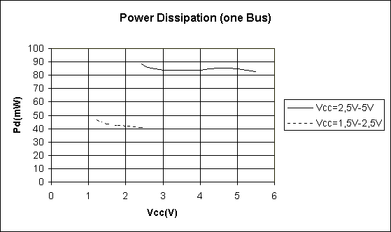
- Figure 5 Power Dissipation (Single Bus)