
Levii Example Transfers
Test Circuit
This page provides information on the transfer behaviour of Levii. The below plots are generated with this test enviroment:
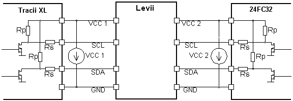
- Figure 1 Test Circuit
The serial resistors Rs do have a value of 22 Ohm, the pull-up resistors Rp are different depending on the actual measurement.
telos Tracii XL2 acts as master while the 24FC32 I2C-RAM is an I2C slave. The transmitted byte is the slave address 0xA0, which causes an acknowledge pulse by the slave.
400 kHz Transfer
The following picture shows an example transfer at an SCL-frequency of 400 kHz. On the left side SCL and SDA of the master and on the right side SCL and SDA of the slave are shown. Both buses use pull-up resistors of 1.6 kOhm and a bus voltage of 5 V.
This figure also points out that the master’s signal uses the entire amplitude while the slave’s signal only drops to a voltage of about 120 mV. This offset voltage is caused by the serial resistances of the lines in addition of Levii’s internal serial resistances and can be observed at every transferred signal.
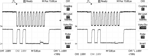
- Figure 2 400 kHz Transfer
400 kHz Shifting Transfer
Figure 3 shows an example transfer with 400 kHz, shifting the bus voltage from 5 V down to 1.8 V. Both sides use pull-up resistors of 1.6 kOhm.
Due to Levi’s symmetric design either side of the device may be connected to the higher voltage.
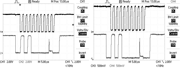
- Figure 3 Shifting Transfer
1 MHz Transfer
Levii is also able to handle I2C speeds higher than the specified maximum of 800 kHz. The figure below shows a part of a successful 1 MHz transfer at bus voltages of 5 V on the master’s and 3.3 V on the slave’s side. The pull-up resistors are 1.6 kOhm at the 5 V and 1.1 kOhm at the 3.3 V interface.
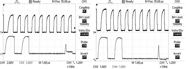
- Figure 4 1 MHz Transfer