
Optii Example Transfers
Test Circuit
The following figures show example I2C transfers generated with the circuit in the figure below.
Test Circuit Image
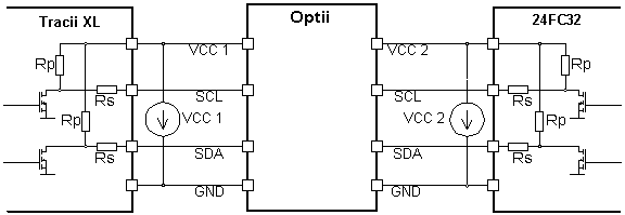
- Figure 1 Test Circuit
The serial resistors Rs do have a value of 22 Ohm, the pull-up resistors Rp are different depending on the actual measurement.
telos Tracii XL 2.0 acts as master while the 24FC32 I2C-RAM is an I2C slave. The transmitted byte is the slave address 0xA0, which causes an acknowledge pulse by the slave.
100 kHz Transfer
Figure 2 shows a 100 kHz transfer with pull-up resistors of 10 kOhm. On the left side the SCL line on channel 1 and SDA on channel 2 of the master is shown while SCL and SDA of the slave is on the right. Both buses use a voltage of 5 V.
At the ninth pulse of SCL, the slave acknowledges its address by actively pulling down its SDA line while the master releases its SDA line. This causes the different offset voltages on both SDA lines.
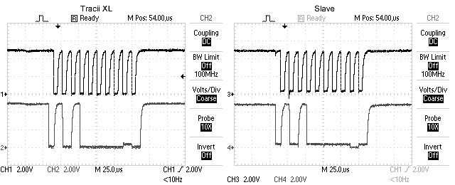
- Figure 2 100 kHz Transfer
400 kHz Transfer
A 400 kHz transfer with level shifting is shown in Figure 3. The left side shows the master at 5 V bus voltage. The right shows the slave with a bus voltage of 1.8 V. Both sides use pull-up resistors of 1.5 kOhm.
The spike at the acknowledge pulse can be led back to the low pull-up resistors in combination with a delay until the slave pulls its line low.
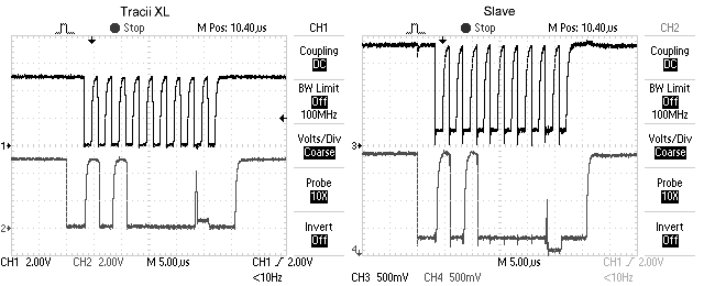
- Figure 3 400 kHz Transfer
1.2 MHz Transfer
Figure 4 shows a SCL pulse of a successful transmission with a frequency of 1.2 MHz. The pull-up resistors were 1.1 kOhm at a bus voltage of 3.3 V (master signal is grey, slave black).
This figure points out the ability of Optii to work with signals faster than the specified maximum of 800 kHz with proper I2C-line parameters (low Rs, Rp and bus-capacitance).
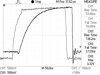
- Figure 4 1.2 MHz Transfer